
PCB Fabrication Process
This page introduces the major steps used in our printed circuit board manufacturing process. From precision drilling and copper plating to inspection and cleanroom handling, our facility is equipped to support both prototype and production PCB fabrication.
By showing real production equipment and process environments, we help customers better understand how we maintain manufacturing consistency, dimensional accuracy, and reliable board quality throughout fabrication.
Overview of Our PCB Manufacturing Capability
Our PCB fabrication workflow includes controlled production environments, automated lines, process-specific equipment, and inspection steps designed to improve manufacturing stability. The images below show real factory operations that support multilayer PCB manufacturing, prototype fabrication, and repeat production orders.
- High precision CNC drilling for multilayer PCB hole formation
- Automated copper plating and electroplating production lines
- Electrical testing and process inspection for quality control
- Cleanroom handling for sensitive manufacturing stages
- Support for prototype, small batch, and production PCB orders
Factory Production Environment
A strong PCB fabrication process begins with a stable manufacturing environment. Our production floor is organized to support continuous workflow, process control, and repeatable board quality for both quick-turn prototypes and volume orders.
PCB Fabrication Factory Production Line
This production area shows the organized factory environment used to support printed circuit board fabrication, throughput, and process coordination.
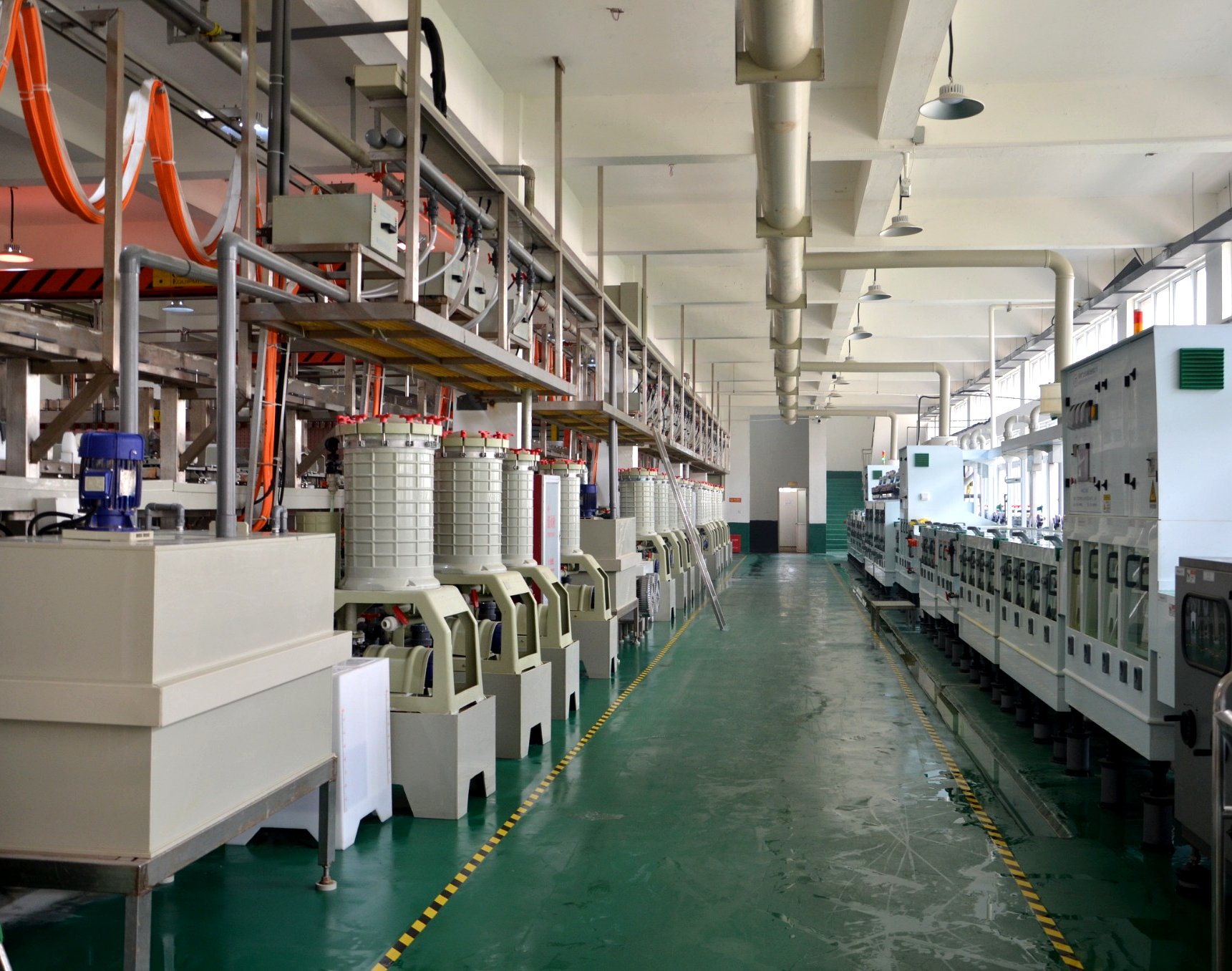
Large Scale Production Environment
Large-format production lines support stable manufacturing flow, organized shop-floor control, and repeatable PCB fabrication capacity for both prototype and repeat production orders.
Drilling Process
Drilling is one of the most important stages in PCB fabrication because it defines the hole structure used for vias, through-holes, and component connections. Precision drilling directly affects registration accuracy and the success of downstream plating operations.
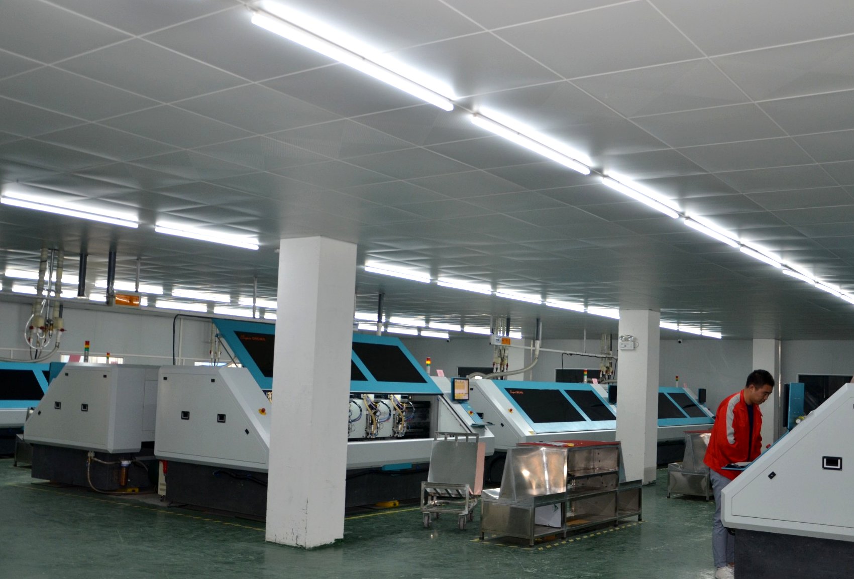
PCB Drilling Production Area
This drilling area shows multiple CNC drilling machines operating in a controlled environment, supporting stable and repeatable PCB fabrication for both prototype and production orders.
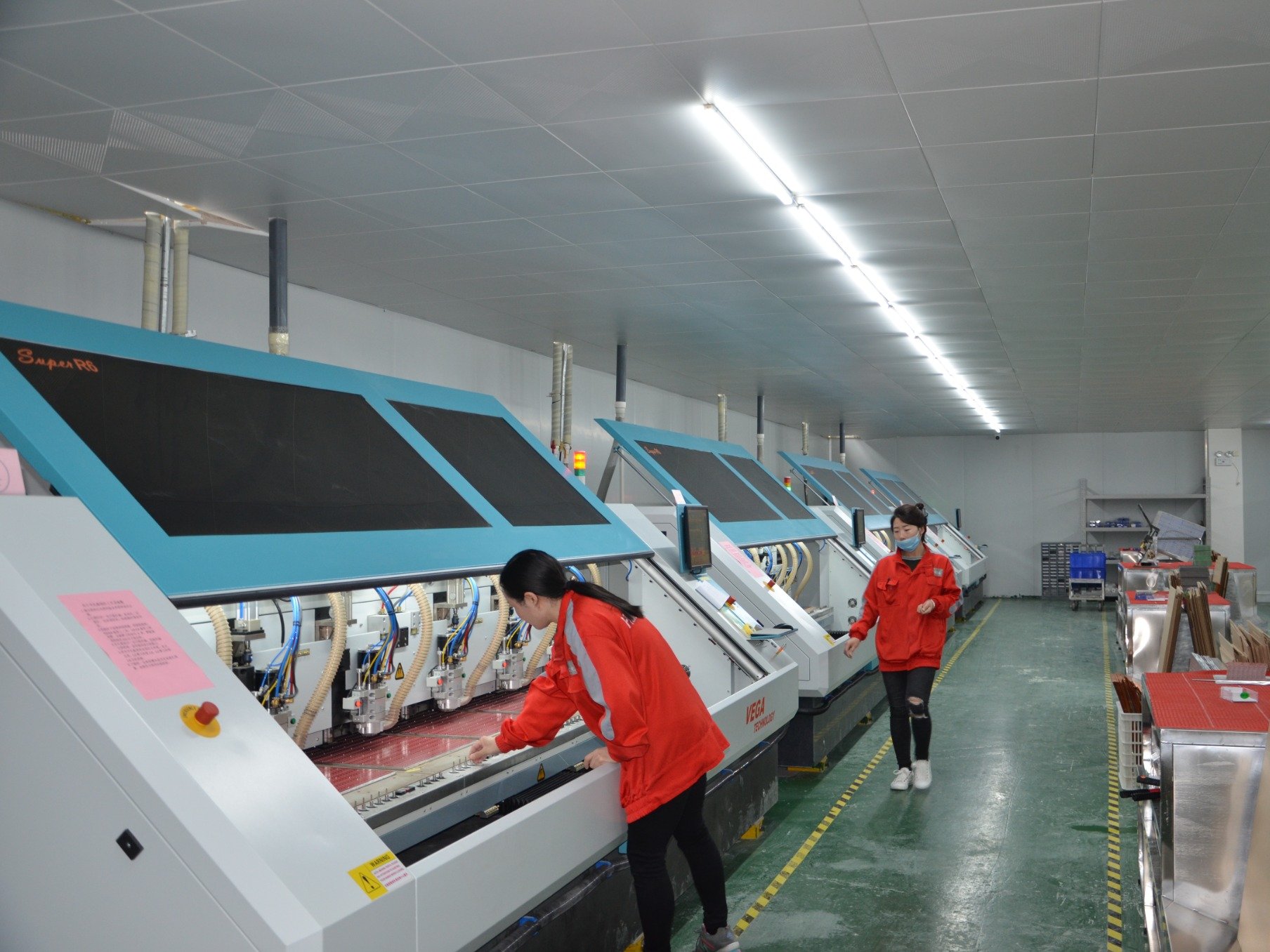
CNC Drilling Machine
CNC drilling equipment is used to create precise hole positions for multilayer PCB fabrication, helping maintain dimensional and interlayer alignment accuracy.
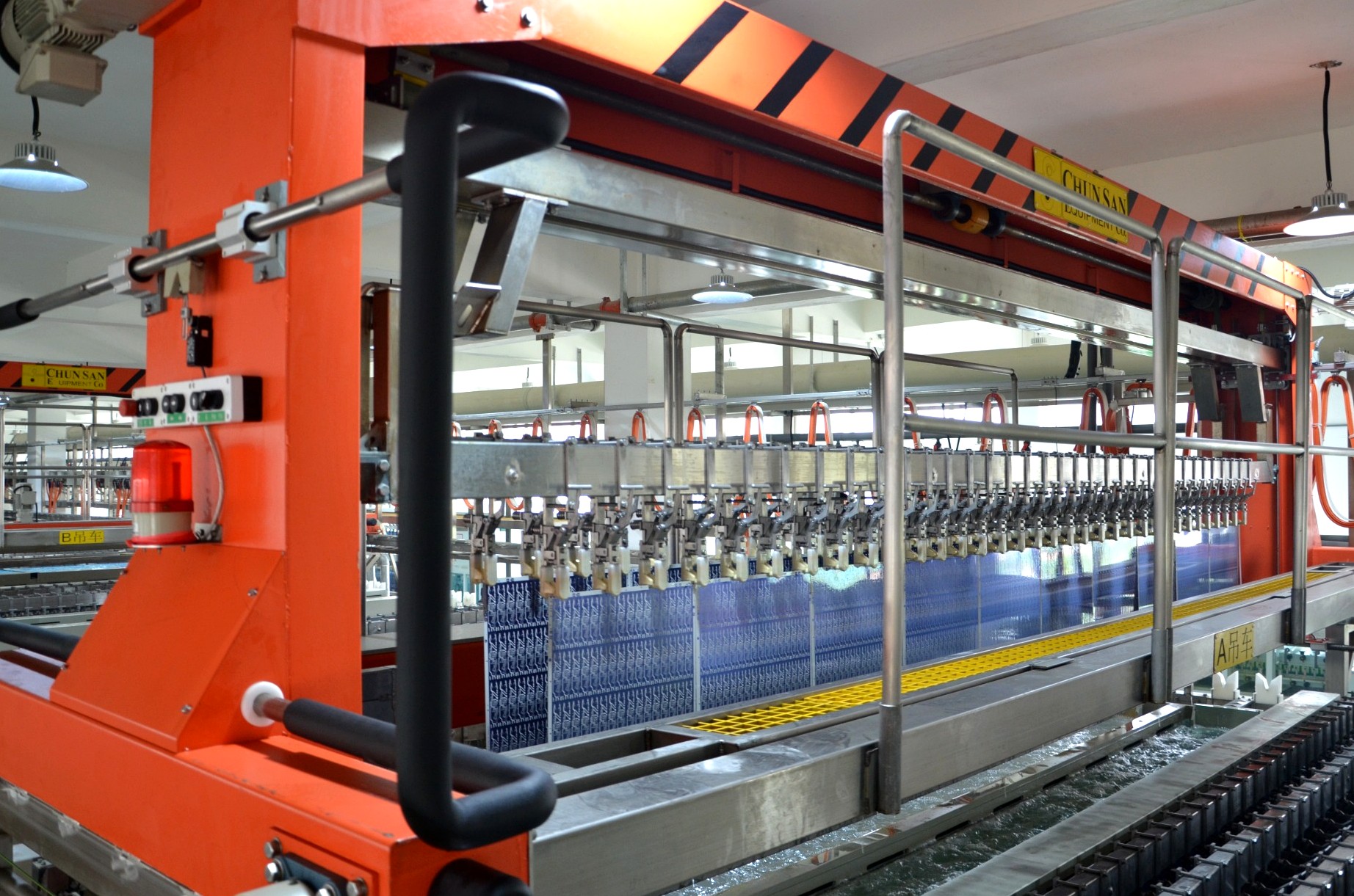
Copper Plating and Electroplating
After drilling, plating processes help establish conductive connections and improve copper coverage inside drilled holes and on board surfaces. Stable plating control is essential for multilayer interconnection reliability and overall PCB performance.
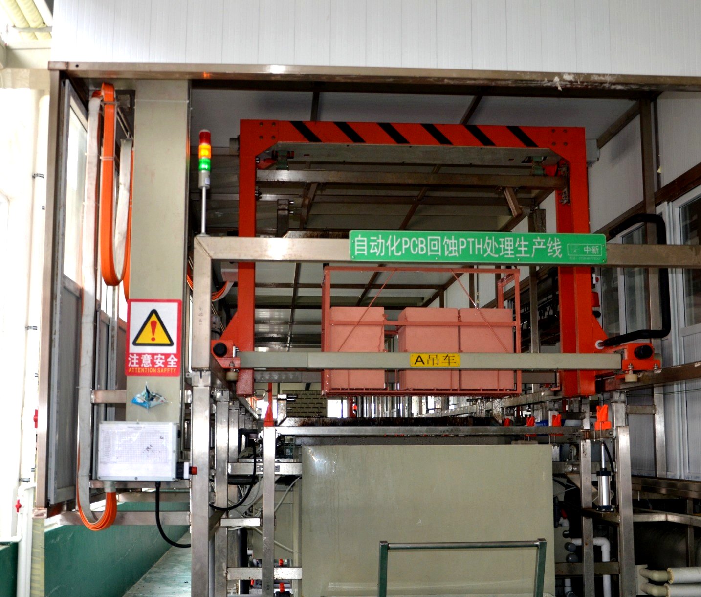
Electroplating Process Line
Copper electroplating is a core part of the PCB manufacturing process and contributes directly to conductive pathway integrity and hole wall metallization.
Inspection and Quality Control
Quality control is built into PCB fabrication, not added afterward. Inspection equipment is used to verify process quality, detect manufacturing deviations, and improve consistency before boards move to later stages or shipment.
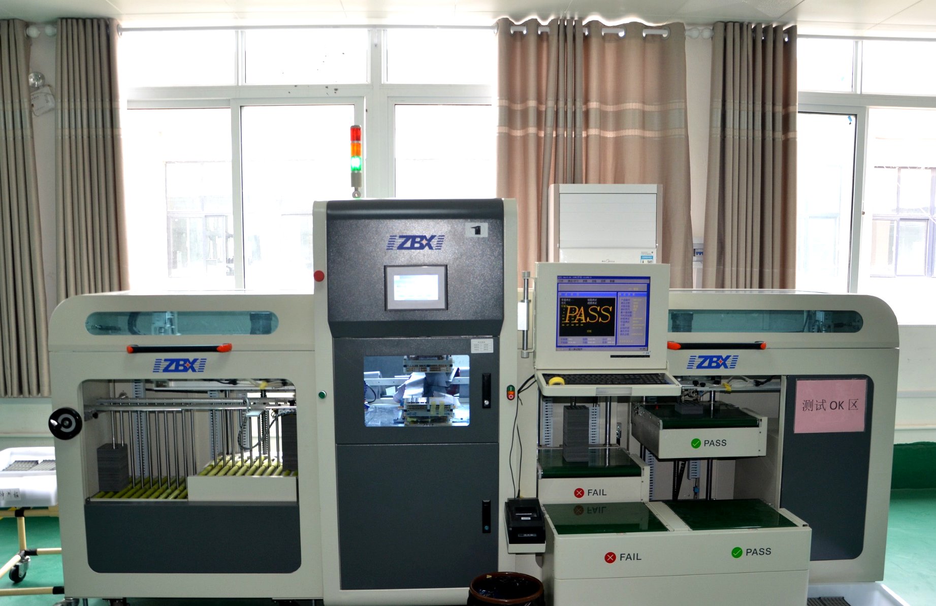
Flying Probe Electrical Test
Flying probe inspection is used to verify electrical connectivity and detect open or short circuit conditions, helping improve PCB quality assurance before shipment.
Cleanroom Handling and Sensitive Process Stages
Some PCB manufacturing operations benefit from cleaner handling conditions to reduce surface contamination and improve process stability. Cleanroom environments and protected operator handling help support more sensitive fabrication steps.
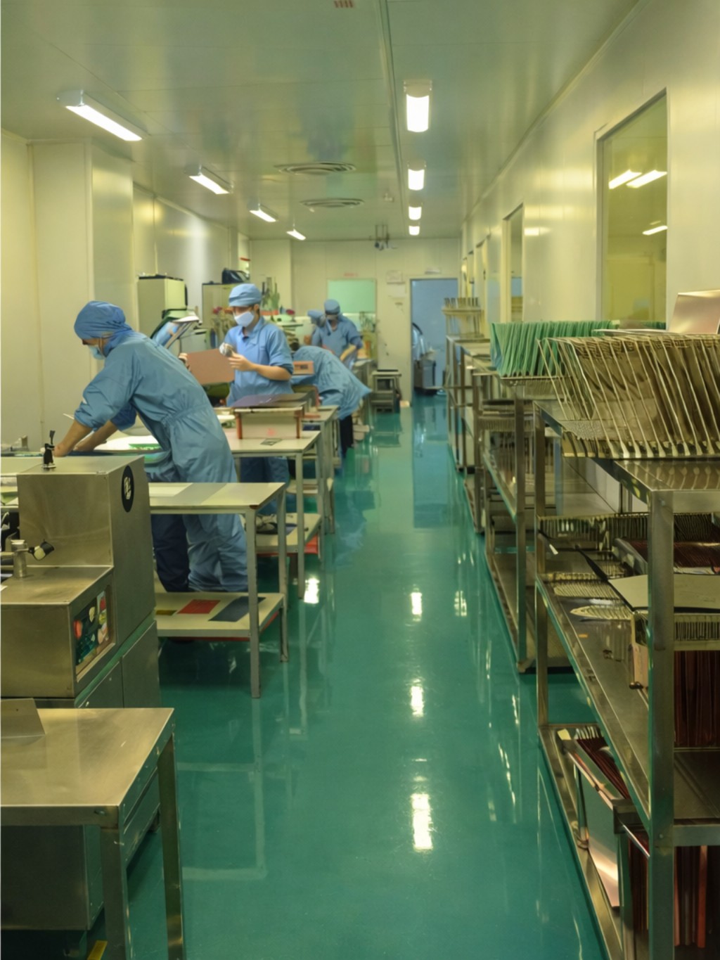
Cleanroom Operator Handling Process
Controlled operator handling in a clean production environment helps reduce contamination risk and supports stable processing for sensitive PCB manufacturing stages.
Need a Quote for PCB Fabrication?
If you are ready to move from process review to quotation, you can request a PCB quote online. You may also review our company page for more details about our experience and manufacturing support.