
Peelable Soldermask PCB
Reliable peelable soldermask PCB fabrication for wave soldering, selective soldering, plating protection, and temporary process masking.

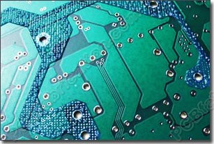
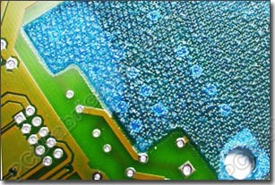
What Is Peelable Soldermask?
Peelable soldermask is a temporary protective coating applied to selected areas of a printed circuit board. It is used to protect pads, holes, contacts, or specific PCB areas during soldering, plating, assembly, or other manufacturing steps.
After the required process is completed, the peelable soldermask can be removed from the PCB. It is designed to have good elasticity, tear resistance, and easy removability.
Why Use Peelable Soldermask?
- Protect selected PCB areas from solder during wave soldering.
- Protect plated holes, gold fingers, contacts, or pads during fabrication or assembly.
- Reduce the need for manual taping or temporary masking.
- Improve process consistency for selective solder protection.
- Support prototype PCB and production PCB manufacturing requirements.
Typical Applications
| Application | Purpose |
|---|---|
| Wave Soldering Protection | Protect selected PCB areas from direct contact with solder during wave soldering. |
| Selective Soldering | Mask areas that should not be soldered during the assembly process. |
| Plating Process Protection | Protect specific areas during PCB surface treatment or plating steps. |
| Contact and Pad Protection | Protect pads, contacts, holes, or exposed copper areas during manufacturing. |
| Temporary Process Masking | Provide removable protection before or after PCB component soldering. |
Benefits of Peelable Soldermask PCB Fabrication
| Benefit | Explanation |
|---|---|
| Temporary Protection | Provides removable protection for selected PCB areas during fabrication or assembly. |
| Easy Removal | The material can be peeled off after the required process is completed. |
| Good Elasticity | Peelable soldermask has elasticity and tear resistance for easier handling. |
| Process Efficiency | Can reduce manual masking work and improve repeatability during PCB manufacturing. |
| Selective Area Protection | Suitable for partial PCB coverage where only specific areas need protection. |
Peelable Soldermask PCB Capability
| Item | Capability |
|---|---|
| Board Type | Single-sided PCB, double-sided PCB, and multilayer PCB |
| Base Material | FR4, High Tg FR4, and other materials upon review |
| Surface Finish | HASL, lead-free HASL, ENIG, OSP, immersion silver, and other options |
| Solder Mask | Standard solder mask plus peelable soldermask in selected areas |
| Order Type | Prototype PCB and production PCB fabrication |
| Required Files | Gerber files, drill files, peelable soldermask layer, drawings, or fabrication notes |
Peelable Soldermask Design Considerations
1. Clearly Mark the Peelable Soldermask Area
The peelable soldermask area should be clearly shown in the Gerber layer, mechanical drawing, or fabrication instruction. Ambiguous marking may delay engineering review and quotation.
2. Avoid Very Small or Complex Shapes When Possible
Peelable soldermask is best suited for areas that can be applied and removed reliably. Very small openings, narrow strips, or complex shapes may require engineering review.
3. Confirm Assembly Process Requirements
If the peelable soldermask is used for wave soldering, selective soldering, or plating protection, please describe the process requirement when requesting the quotation.
4. Review Removal and Residue Requirements
Peelable soldermask is intended to be removed after the required process. If your application has special cleanliness, residue, or assembly requirements, please inform us before production.
Peelable Soldermask PCB Quote
To request a peelable soldermask PCB quotation, please send your Gerber files, drill files, board quantity, material requirement, surface finish, solder mask color, and peelable soldermask location details.
Peelable soldermask PCB requires engineering review. Please contact us and send your Gerber files, drawings, and peelable soldermask location details.
Contact Us for Peelable Soldermask PCB
Peelable Soldermask PCB FAQ
What is peelable soldermask used for?
Peelable soldermask is used to temporarily protect selected PCB areas during soldering, plating, assembly, or other manufacturing processes.
Can peelable soldermask be removed after soldering?
Yes. Peelable soldermask is designed to be removed after the required soldering or manufacturing process is completed.
How should I show peelable soldermask in the Gerber files?
The required peelable soldermask areas should be clearly marked in a dedicated Gerber layer, drawing, or fabrication note.
Is peelable soldermask available for prototype PCB orders?
Yes. Peelable soldermask can be reviewed for prototype PCB and production PCB orders.
Can peelable soldermask be used with ENIG surface finish?
Peelable soldermask can be reviewed with common surface finishes such as HASL, lead-free HASL, ENIG, OSP, and immersion silver.